Athena Simulation and Code Analysis of a Simple CMOS Structure
Simulation
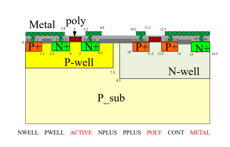
For the final project, we used Athena to create a CMOS manufacturing process. The structure is shown below.
Simulation results:
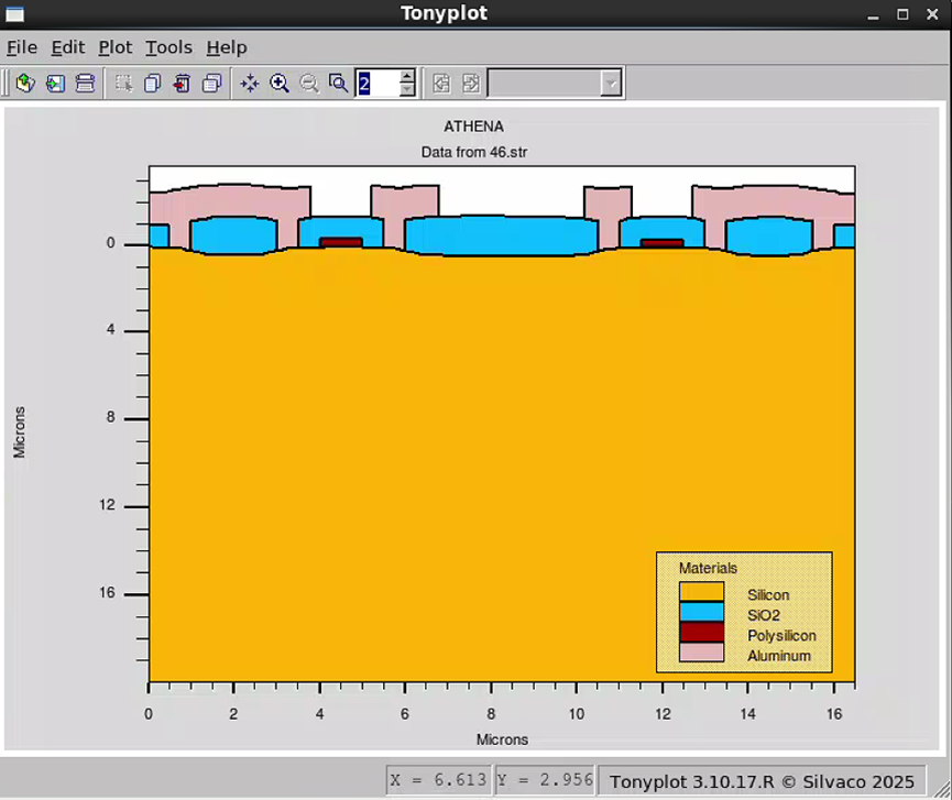
Simulation Data:
Extracted parameters(The data must be clearly given, and the screenshots are needed for prove)
The step 5, extract the nwell junction depth 05nwell = 0.742309um
The step 7, extract the thickness of SiO2 inside Nwell 07tox_in_nwell = 0.210375um
The step 7, extract the thickness of SiO2 outside Nwell 07tox_out_nwell = 0.243607um
The step 7, step height of silicon surface = 0.178331-0.114659 um = 0.063672um
The step 7, extract the junction depth of Nwell 07nwell = 4.45937um
The step 9, extract the thickness of SiO2 inside Nwell 09tox_in_nwell = 0.0430882um
The step 9, extract the thickness of SiO2 outside Nwell 09tox_out_nwell = 0.0430863um
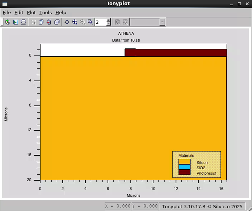
Step 10, observe the photoresist
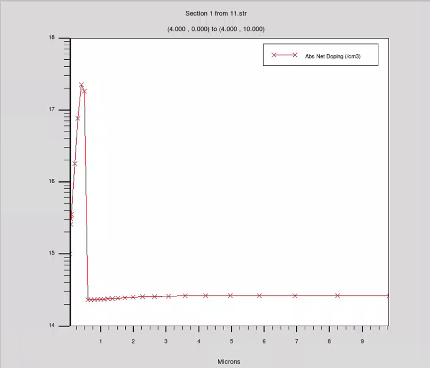
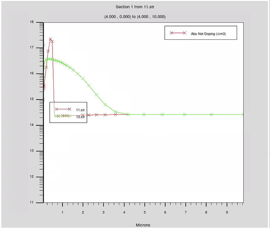
Step 11, curve of Boron concentration, x axis for 1D curve range 0-10
Step 13, plot curve1 and 2 in one picture x axis range 0-10
The step 15, extract thickness of SiO2 in the active region 15thickness_of_SiO2_in_active_region = 0.0421572um
The step 20, extract thickness of SiO2(X.val=8) 20SiO2 = 0.951967um
The step 22, due to the step 20, thickness of SiO2 needs to be etched is about 0.15um, extract remained thickness of SiO2 22SiO2 = 0.801967um
The step 23, extract thickness of SiO2 X=4.5 23SiO2 = 0.0335531um
The step 28, thickness of oxide on top of NMOS Poly and PMOS Poly 28NpolySiO2 = 0.0125231um 28PpolySiO2 = 0.0125231um
The step 31, extract junction depth of N+, x = 3.5 31N+1 = 0.266465um, x = 5.5 31N+2 = 0.265963um
The step 33, extract thickness of oxide on top of NMOS Poly and PMOS Poly 33Npoly = 0.0200301um 33Ppoly = 0.0322859um
The step 36, extract junction depth of P+, x = 11 36P+1 = 0.303582um, x=13 36P+2 = 0.29539um
The step 47,
1. Vt for NMOS with Vsub=2V; 47NVt = 2.48013V
2. Vt for PMOS with Vsub=0V; 47PVt = -1.6258V
3. Channel doping for NMOS and PMOS; 47NChannelDoping = 2.71413e+15 atoms/cm3, 47PChannelDoping = 1.47776e+16 atoms/cm3.
4. Gate oxide thickness for NMOS and PMOS 47Noxide = 0.0335536um, 0.0335637um.
Below is my simulation code:
This code simulates a typical CMOS manufacturing process, starting from the initial silicon substrate, going through a series of steps including doping, oxidation, etching, and deposition, ultimately forming transistor structures with basic functionality.
Code Analysis
Let us analyze the key parts of the code step by step:
1. Preparation Phase (#00, #01)
go athena: Launches the Athena process simulator.line: Defines the 2D simulation region and mesh density. Note that the surface should have higher density.init silicon boron resistivity=50 orientation=100 two.d: Initializes the simulation substrate. We start with a boron-doped (P-type), 50 ohm-cm resistivity, (100)-oriented silicon substrate. This is the most common CMOS starting material.
2. N-Well Formation (#02 - #08)
deposit oxide thick=0.1: Deposits a thin oxide layer, which may serve as a buffer or sacrificial layer for subsequent implantation.deposit photoresist thick=1.2: Deposits photoresist.etch photoresist right p1.x=8.5: Etches away the photoresist to the right of coordinate x=8.5. The photoresist on the left is retained, forming a mask.etch oxide: Etches away the exposed oxide layer beneath (to the right of) the photoresist.implant phosphor dose=5.0e12 energy=130 crystal: Implants phosphorus in the exposed region. Phosphorus is an N-type dopant. This implantation forms an N-type region within the P-type substrate, i.e., the N-well. The dose and energy determine the concentration and depth of the implant. Thecrystalparameter indicates that crystal effects are considered.extract name="05nwell" xj ...: Measures the junction depth (xj) of the N-well after implantation.etch photoresist all: Removes the remaining photoresist.diffus ...: A series of long, high-temperature diffusion steps follow, with temperatures rising from 800°C to 1180°C under various atmospheres (O2, N2). The purposes of these steps are:- Activating the implanted phosphorus to make it electrically active.
- Diffusing phosphorus atoms deeper into the silicon and laterally, forming a deeper and wider N-well.
- Oxide growth may accompany the process where O2 is present.
extract ...: After diffusion, measures the N-well junction depth, oxide thickness, and other parameters again to check the diffusion results.etch oxide all: Removes oxide layers generated or remaining after diffusion.
3. Field Oxide (LOCOS) Formation (#09 - #21)
diffus ...: Another series of diffusion steps, possibly used to grow a thin pad oxide layer.deposit nitride thick=0.15: Deposits a silicon nitride layer. Nitride blocks oxygen diffusion during high-temperature oxidation and is commonly used as a mask for local oxidation (LOCOS).etch nitride start ... done ...: Using precisely defined coordinates, etches away the nitride layer, exposing the underlying structure in areas where transistor "active regions" will be formed. The un-etched nitride regions correspond to future "field regions" where thick isolation oxide will grow.diffus ... f.h2=7.3 f.o2=4: Long high-temperature diffusion (950°C). Note thef.h2andf.o2parameters, representing a wet oxygen ambient—a typical field oxidation process condition. In areas not masked by nitride, the silicon undergoes extensive oxidation, forming a thick field oxide (FOX) layer used to isolate different devices.extract ...: Measures the field oxide thickness.etch nitride all: Removes the remaining nitride mask.
4. Gate Formation (#22 - #26)
etch oxide dry thick=0.15: Etches away part of the oxide layer, likely to clean the surface in active regions.diffus ... dryo2: Short high-temperature (1000°C) dry oxygen diffusion. This is the key step for growing a thin gate oxide. The gate oxide is the insulating layer between the gate electrode and the silicon substrate.extract ...: Measures the gate oxide thickness.deposit polysilicon thick=0.35 c.phosphor=5e12: Deposits a phosphorus-doped (N-type) polysilicon layer. Polysilicon is the commonly used gate electrode material in modern CMOS devices.etch polysilicon start ... done ...: Etches the polysilicon layer to form independent gate structures.
5. Source/Drain Formation (#27 - #37)
diffus ...: Short annealing steps, possibly used to stabilize the gate or grow a thin passivation oxide.extract ...: Measures the oxide thickness on top of the polysilicon.init infile=28.str: Reads the structure file saved from the previous step, ensuring the next step starts from the correct state.deposit photoresist thick=1.2: Deposits photoresist.etch photoresist start ... done ...: Etches the photoresist, exposing regions where N+ source/drain will be formed. Note that the gate polysilicon also serves as a mask (self-aligned process).implant arsenic dose=5.0e15 energy=80 crystal: Implants arsenic. Arsenic is an N-type dopant with a very high dose (5e15), used to form heavily doped N+ regions. This forms the NMOS source/drain regions on either side of the gate in the P-type substrate (left-side region).extract ... xj ...: Measures the N+ source/drain junction depth.etch photoresist all: Removes the photoresist.diffus ...: Annealing steps to activate the N+ doping.deposit photoresist ... etch photoresist ...: Deposits and etches photoresist again, exposing regions where P+ source/drain will be formed.implant bf2 dose=4.0e15 energy=80 crystal: Implants BF2. After BF2 dissociates, boron is implanted. Boron is a P-type dopant. This forms the PMOS P+ source/drain regions on either side of the gate in the N-well region (right-side region).extract ... xj ...: Measures the P+ source/drain junction depth.etch photoresist all: Removes the photoresist.
6. Interconnect Formation (#38 - #46)
deposit oxide thick=1: Deposits a thick oxide layer serving as the interlayer dielectric (ILD) to isolate the metal layer from the underlying structures.etch oxide start ... done ...: Etches contact holes, exposing the source/drain regions and gate areas that need to be connected to metal.deposit aluminum thick=1.45: Deposits an aluminum layer. Aluminum is a common metal interconnect material.etch aluminum start ... done ...: Etches the aluminum layer to form metal interconnects, connecting to the underlying source/drain and gate through the contact holes.
7. Parameter Extraction and Analysis (#47)
extract name="47NVt" 1dvt ntype vb=2.0 x.val=4.5: Extracts the threshold voltage (Vt) of the NMOS transistor (near x=4.5) under a given substrate bias.extract name="47PVt" 1dvt ptype vb=0 x.val=12: Extracts the threshold voltage of the PMOS transistor (near x=12).extract name="47NChannelDoping" surf.conc ...: Extracts the surface net doping concentration in the NMOS channel region.extract name="47PChannelDoping" surf.conc ...: Extracts the surface net doping concentration in the PMOS channel region.extract name="47Noxide" thickness ...: Extracts the gate oxide thickness beneath the NMOS gate.extract name="47Poxide" thickness ...: Extracts the gate oxide thickness beneath the PMOS gate.
These extracted parameters are key indicators for evaluating whether the simulation results meet design specifications.
Summary
Through this Athena code of less than 300 lines, we have simulated the core CMOS manufacturing flow: N-well formation, field oxide isolation, gate fabrication, source/drain implantation and annealing, and finally metal interconnects. Each command corresponds to an actual process step in a semiconductor fabrication facility.
The structure outfile=XX.str commands in the code save the current structure file after each step. These files can be opened in DeckBuild, Athena's visualization tool, to observe how the device structure evolves as the process progresses—such as dopant region diffusion, oxide layer growth, etched patterns, and more.
Process simulation is an indispensable part of modern integrated circuit design and manufacturing. It not only helps engineers understand complex physical and chemical processes and predict the impact of process variations on device performance, but also enables extensive experimentation and optimization before committing to expensive actual production, significantly shortening development cycles and reducing costs.
Comments