Designing and Simulating a 6×6 Array Multiplier in Cadence
Background
The multiplier is a core arithmetic unit in digital ICs, and its performance directly impacts overall system efficiency. In VLSI design, array multipliers are widely adopted for their regular structure and straightforward implementation.
In this project, we completed the full front-end and back-end design of a 6×6-bit array multiplier based on 0.18μm CMOS process with 1.8V supply — from transistor-level circuitry and standard cell library construction, to layout drawing, DRC/LVS verification, and post-layout simulation performance evaluation. The entire flow was fully executed.
Design Highlights
1. Transistor Sizing Optimization
Through parametric sweeps (NMOS width 0.4μm~2.0μm, 20 linear steps), the optimal trade-off point was identified on the area×delay product curve. The final sizing: PMOS width-to-length ratio (W/L)p = 2.5×(W/L)n, PMOS width uniformly 1.25μm, NMOS 0.5μm, channel length 0.18μm for both.
2. Standard Cell Library Design
A complete library of four basic gates — INV, NAND, NOR, XOR — was built, with AND and OR gates cascaded from them. All cells use multi-finger structures to ensure consistent layout height, achieving an extremely compact floorplan.
Gate propagation delays (post-layout simulation, Cout=15fF):
- INV: tPLH=0.0926ns, tPHL=0.1112ns
- NAND: tPLH=0.0825ns, tPHL=0.1283ns
- XOR: tPLH=0.2221ns, tPHL=0.2119ns
- NOR: tPLH=0.1164ns, tPHL=0.1110ns
3. Custom 24T Full Adder
A 24-transistor full adder was designed, with the output inverter removed to reduce transistor count and power consumption. The inverted output signal is naturally compatible with the multiplier array architecture. Two complementary half-adders (XOR+OR and XOR+NAND) were used to flexibly control carry signal polarity, further reducing the number of inverters required.
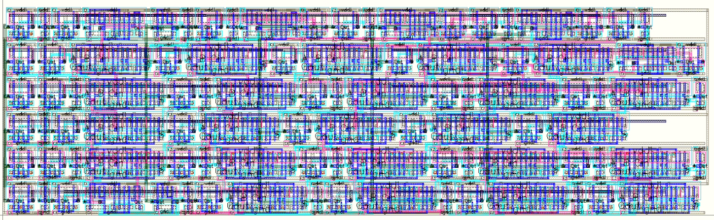
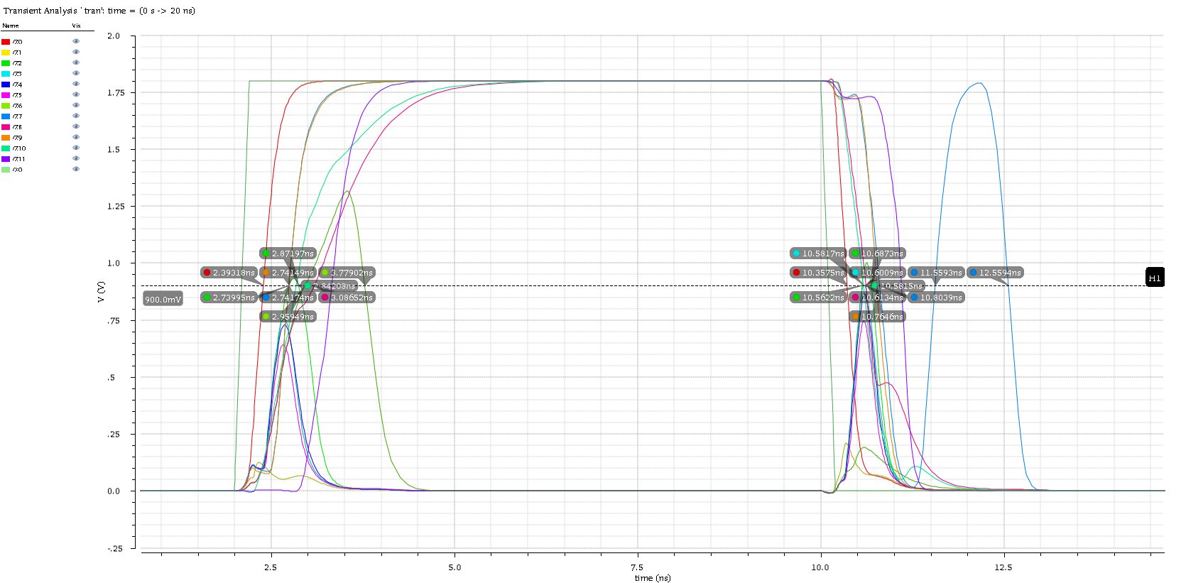
Layout and Performance
The complete layout occupies only 104.892 × 30.961 = 3247.56 μm², and successfully passed both DRC and LVS verification.
| Metric | Schematic Simulation | Post-Layout Simulation |
|---|---|---|
| tPLH | 0.8177 ns | 1.2245 ns |
| tPHL | 0.6368 ns | 1.0014 ns |
| Layout Area | 3247.56 μm² | |
| Total Transistors | 852 | |
Post-layout delay is approximately 1.5× that of pre-layout simulation. The difference primarily arises from parasitic resistance in metal interconnects and inter-layer coupling capacitance in the actual layout — effects that cannot be captured in idealized schematic simulation.
Resource Statistics
The optimized 6×6 array multiplier architecture uses only:
- 24 INV inverters
- 40 NAND gates
- 2 NOR gates
- 6 XOR gates
- 24 24T full adders
- Total: 852 transistors
Summary
This project walked through the complete digital CMOS IC design flow: architecture design → transistor-level circuit → schematic simulation → layout drawing → DRC/LVS → parasitic extraction → post-layout simulation. Through careful trade-offs between area and delay, the final design achieved excellent performance among its class.
📥 Project File Download
Complete Cadence project files can be downloaded here:
🔗 Click to Download Project Files
⚠️ Files are encrypted — leave a comment for the password~
💬 Have questions or want to discuss IC design? Feel free to leave a comment!
Comments