Cyber Junqi: Electronic Military Chess PCB Design with Circuit-Based Arbitration
In an analog integrated circuit course, we used JLCPCB EDA to design a complete electronic military chess game from schematic to layout—embedding the arbitration logic of a traditional board game directly into a PCB, enabling automatic piece comparison and turn-order determination. The project received a perfect score and ranked first in the class.
1. Where Did the Idea Come From?
Military chess has a pain point in its hidden-piece mode: when two pieces collide, a third party (referee) is needed to check ranks and determine the winner. If there are only two players, they must either take turns acting as referee (compromising fairness) or play with revealed pieces (losing the fun of hidden play).
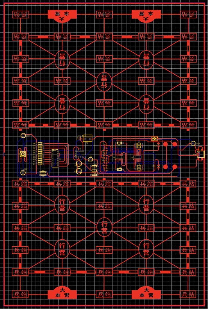
Could a circuit serve as the referee? That's how Cyber Junqi was born—each piece has electronic contacts on its underside; when placed on the board, ranks are automatically compared, and LEDs directly indicate the winner. Two players can start a game anywhere, with absolutely no need for a third person.
2. Core Design: Resistor-Encoded Automatic Comparison
The idea is simple: each piece has a resistor of a different value soldered to its underside, encoding the piece's rank via resistance.
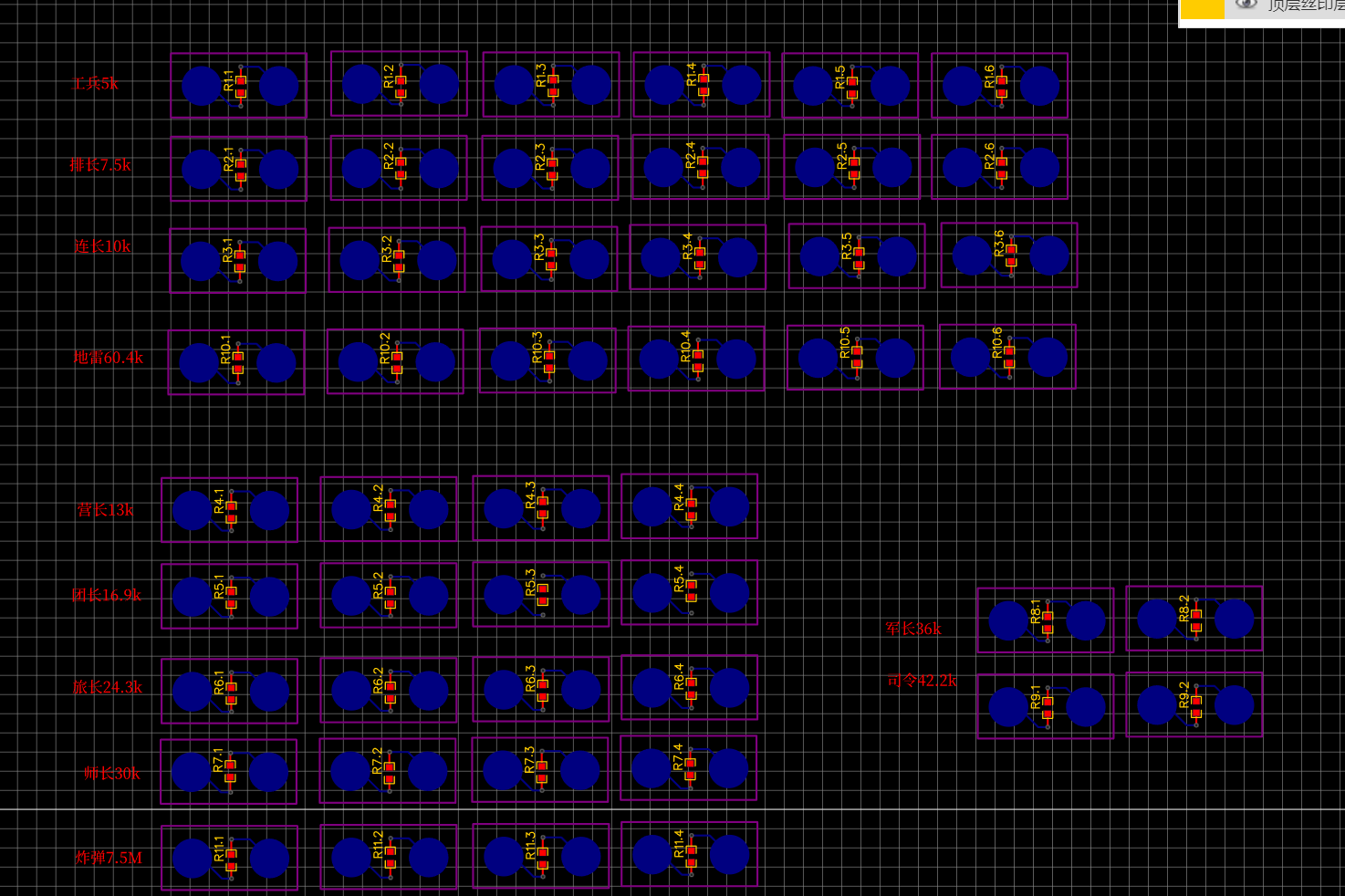
| Piece Rank | Encoding Resistor | Piece Rank | Encoding Resistor |
|---|---|---|---|
| Sapper | 5 kΩ | Colonel | 16.9 kΩ |
| Lieutenant | 7.5 kΩ | Brigadier | 24.3 kΩ |
| Captain | 10 kΩ | Division Commander | 30 kΩ |
| Major | 13 kΩ | Army Commander / Commander-in-Chief | 42.2 kΩ |
| Landmine (60.4 kΩ, only defeated by Sapper) | Bomb (7.5 MΩ, mutually destroys with any piece) | ||
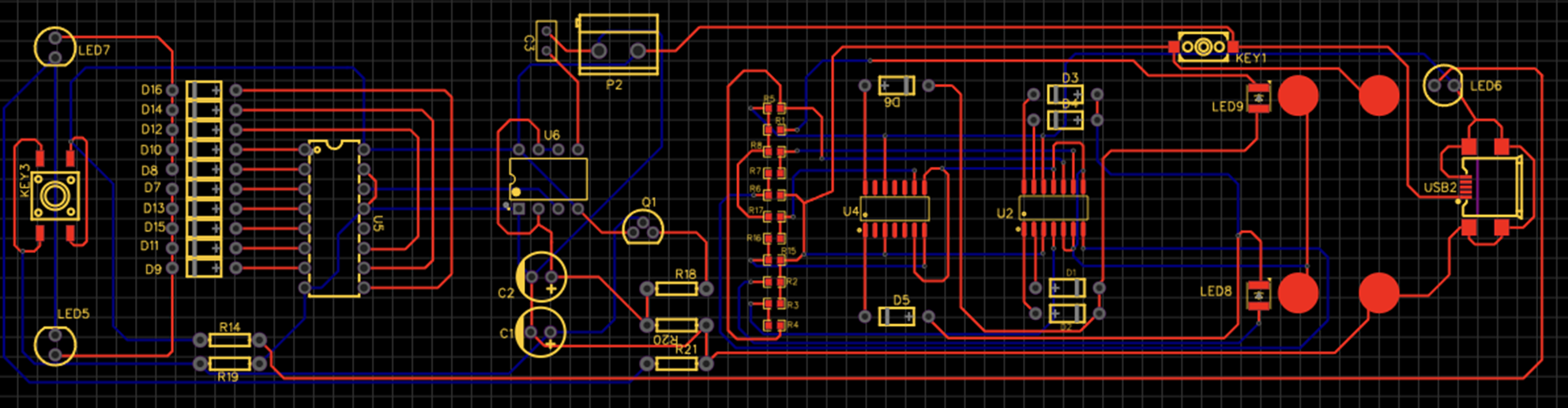
The board contains a comparator circuit: when two pieces contact the board, the circuit reads both resistance values → compares them → LEDs indicate the winner. There is also a logic circuit that automatically determines turn order.
3. From Schematic to Finished Product
The entire design process was completed in JLCPCB EDA:
- Schematic Design: The comparison circuit (comparator + resistor network) and turn-order circuit (D flip-flop + LED driver) were designed as two independent sections
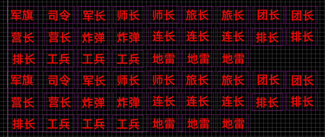
- PCB Layout: The board follows the standard military chess board pattern, with electronic contacts placed at camp/station positions; piece undersides use copper pads as contact interfaces—no plugging/unplugging needed
- Gerber Output: Three sets of Gerber files were exported separately—the board, piece undersides, and piece fronts—for PCB fabrication
Special attention was given to user experience in piece design: the underside uses contact-type copper pads rather than pins—press to connect, lift to disconnect, providing smooth and natural operation. The front silkscreen labels the rank for easy identification.
4. Highlights and Takeaways
"Compiling" traditional game rules into circuit logic was the most fascinating part of this project. The military chess rank chain (Commander-in-Chief > Army Commander > ... > Sapper) maps naturally to a linear comparison of resistor values; the Bomb's special rule (mutual destruction with any piece) is triggered via an extremely high resistance (7.5MΩ); the Landmine's partial immunity (only defeated by Sapper) is implemented using resistance range detection.
This was not merely a PCB design exercise—it was a complete reflection on how analog circuits solve real-world problems: from requirements analysis and solution selection to schematic design, layout, BOM compilation, and Gerber export, the entire hardware productization workflow was carried out end-to-end.
The project was designed using JLCPCB EDA. Gerber files and BOM are archived and can be used directly for replication.
Comments