From Five-Stage Pipeline to VLIW: ARMv3 Processor Microarchitecture Design and FPGA Verification
In the microprocessor design course, our four-person team built a complete ARMv3 architecture processor from scratch—from a five-stage pipeline and Cache subsystem to a floating-point unit, and finally extending to a VLIW dual-issue architecture, all with board-level verification on the Nexys A7 FPGA.
1. Project Overview: More Than Just "Building a CPU"
This is not a simple single-cycle CPU course lab. The entire project is divided into eight progressive modules covering the core technology stack of modern processor design:
- Q1 · Five-Stage Pipeline + Hazard Handling: Decomposed the single-cycle ARMv3 into IF→ID→EX→MEM→WB five-stage pipeline, implementing Forwarding and Stalling to resolve data/control hazards
- Q2 · Non-blocking Multi-cycle Instruction Execution: Extended data dependency detection and pipeline interlocks for long-latency instructions such as MUL/DIV
- Q3 · All 16 Data Processing Instructions: ALU hardware reuse design, supporting ADD/SUB/AND/ORR/MOV/MVN and all other ARM data processing instructions with minimal logic resources
- Q4 · 4-Way Set-Associative Cache: 4KB Cache, Write-Allocate + Write-Back strategy, LRU replacement algorithm — my primary contribution
- Q5 · IEEE 754 Floating-Point Unit: Complete FPU supporting floating-point add/subtract/multiply/divide, handling edge cases such as NaN and infinity
- Q6 · Single-Cycle RISC-V Processor: Comparing ARM architecture differences, implementing the RV32I instruction set
- Q7 · RISC-V Five-Stage Pipeline: Pipelining the RISC-V version, completing hazard handling
- Bonus · VLIW Dual-Issue Architecture: Statically scheduled Very Long Instruction Word architecture, executing two instructions in parallel per cycle — my primary contribution
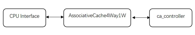
2. Cache Subsystem: 4-Way Set-Associative + LRU Replacement
The performance bottleneck of modern processors is not the CPU core but the memory wall. The quality of Cache design directly determines system throughput. We implemented a 4KB 4-way set-associative Cache, organized as 256 lines × 4 ways × 4 bytes, using Write-Allocate (load the block first on a write miss, then write) and Write-Back (dirty blocks written back to memory only upon eviction) strategies.
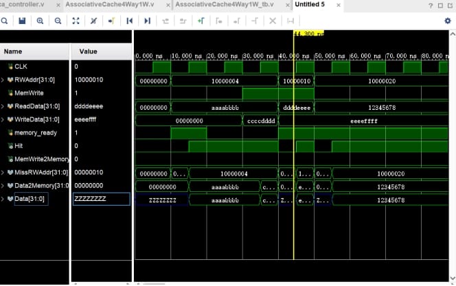
Address Partitioning and Hit Detection
The 32-bit address is divided into Tag (22 bits), Index (8 bits), and Offset (2 bits). Each way independently maintains a Valid Bit, Dirty Bit, and 22-bit Tag:
LRU Replacement Algorithm
After each Cache access, the LRU priority markers for the four ways of that line are updated. When a replacement is needed, the way with the highest LRU value (least recently used) is selected for eviction. The design specifically addresses sorting errors caused by LRU counter overflow—by limiting the LRU increment to 1 and resetting only on a hit to 0, ensuring correct ordering even after an unlimited number of hits.
3. VLIW: Making the Processor "Do Two Things at Once"
Superscalar processors rely on hardware dynamic scheduling to achieve instruction-level parallelism—this requires complex out-of-order execution logic and significant silicon area. VLIW (Very Long Instruction Word) takes a different path: shifting the scheduling responsibility to the compiler, with hardware needing only the simplest dual-issue controller.
In our design, we instantiate two independent ARM Core instances within the VLIW module, distributing instructions through PC interleaving—ARM0 executes even-numbered lines, ARM1 executes odd-numbered lines—achieving simultaneous issue of two dependency-free instructions per cycle.
The test code simultaneously issues ADD/SUB/AND instruction pairs, using two independent register sets (R0-R7 and R8-R15) to avoid data dependencies:
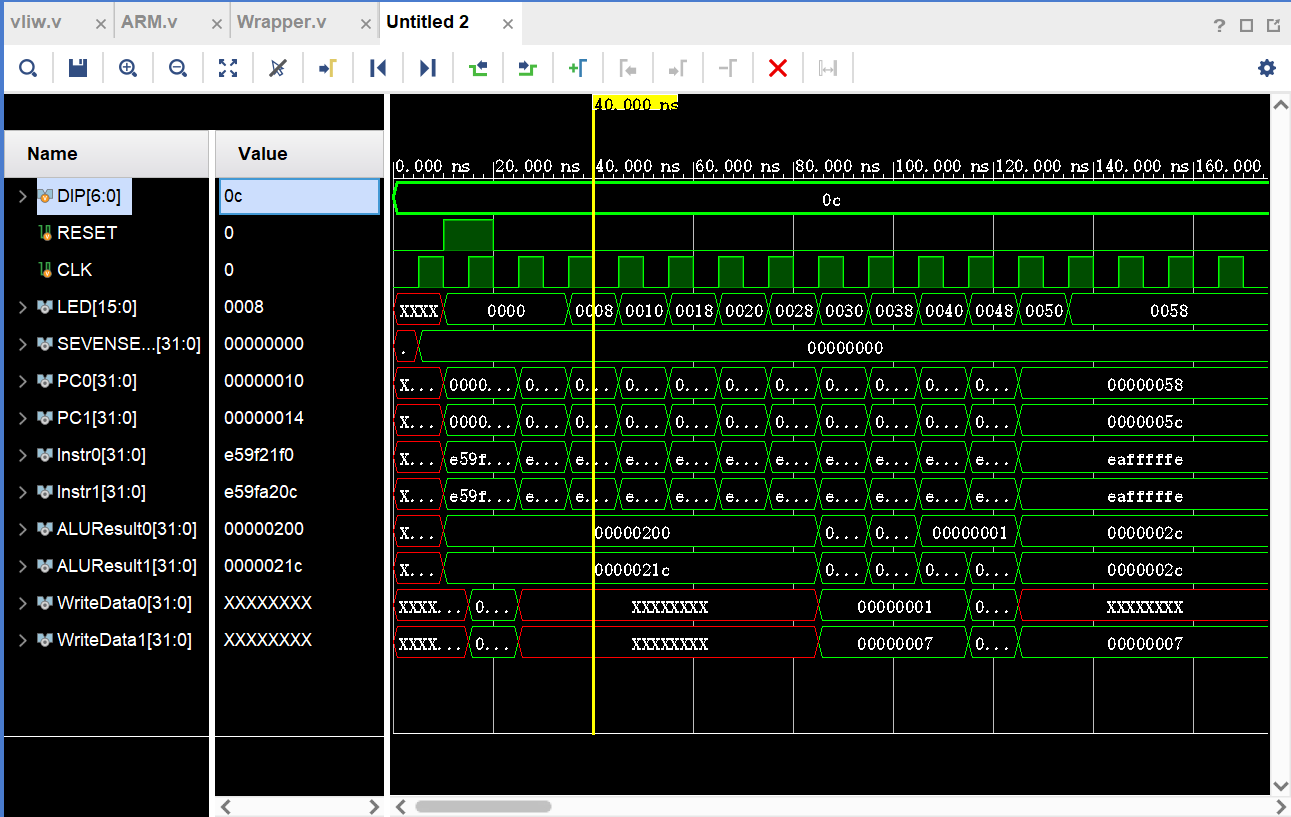
Test result: 16 instructions completed in only 8 cycles, doubling efficiency compared to a single-issue processor. This verifies that the VLIW architecture can achieve near-linear speedup with sufficient compiler scheduling.
4. From Simulation to Real Hardware
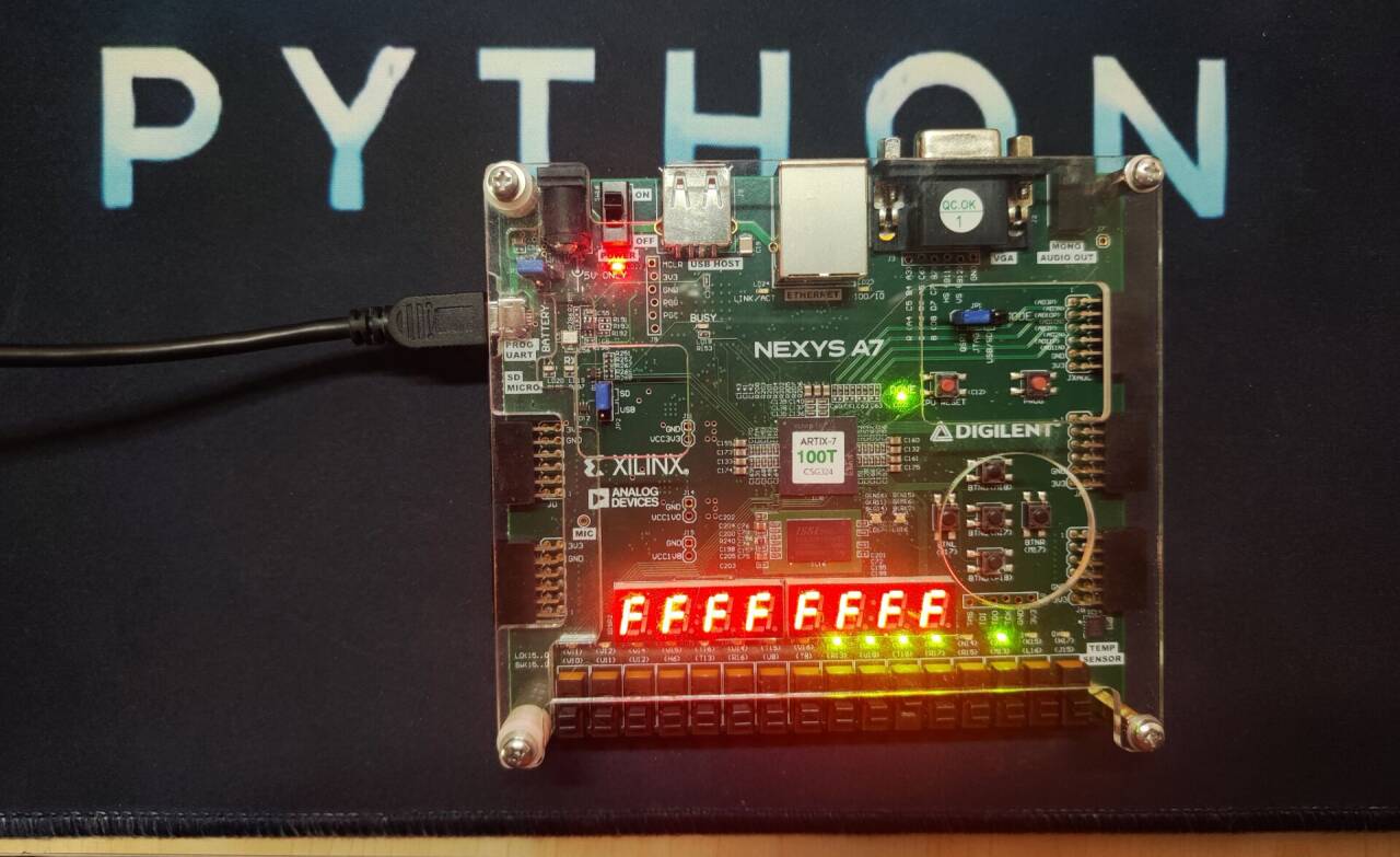
All modules underwent the complete flow of Verilog simulation → Synthesis → Place & Route → Bitstream programming and verification. On the Nexys A7 (Xilinx Artix-7 100T) FPGA, we completed board-level testing of the ARMv3 five-stage pipeline, Cache, FPU, and RISC-V processor—DIP switches for instruction input, LEDs and seven-segment displays for result output, and VGA for waveform display.
This is not merely a course assignment but a complete practice of the full processor microarchitecture design flow: from instruction set understanding and pipeline hazard analysis to memory hierarchy design and instruction-level parallelism exploration—each step answers the fundamental question of "how a computer works."
Comments