High-Performance CMOS Operational Amplifier Design Using the gm/ID Methodology
Key Results: Based on 0.18μm CMOS technology, a high-performance op-amp was realized with under 500μW power consumption, achieving 63dB gain, 149MHz bandwidth, and 152V/μs slew rate—all specifications significantly exceeding the design requirements.
Why the gm/ID Methodology?
What is the most frustrating aspect of analog IC design? — Sizing transistors. The traditional approach relies on square-law hand-calculation formulas, but in deep submicron processes, non-ideal factors such as short-channel effects and velocity saturation make these formulas increasingly unreliable. Iterative simulation and blind parameter tuning have earned the industry nickname "SPICE Monkey".
The gm/ID methodology provides a thorough solution. It does not rely on idealized formulas but instead uses characteristic curves generated from real process library simulations, directly mapping device physics to circuit performance.
The design flow becomes clear: starting from the GBW specification, determine gm → consult curves to select channel length L → select gm/ID value → calculate ID → consult Id/W curve to obtain W. A single iteration yields reasonable sizes, completely eliminating blind tuning.
Approach 1: Two-Stage Op-Amp — 5T-OTA + Common-Source Output
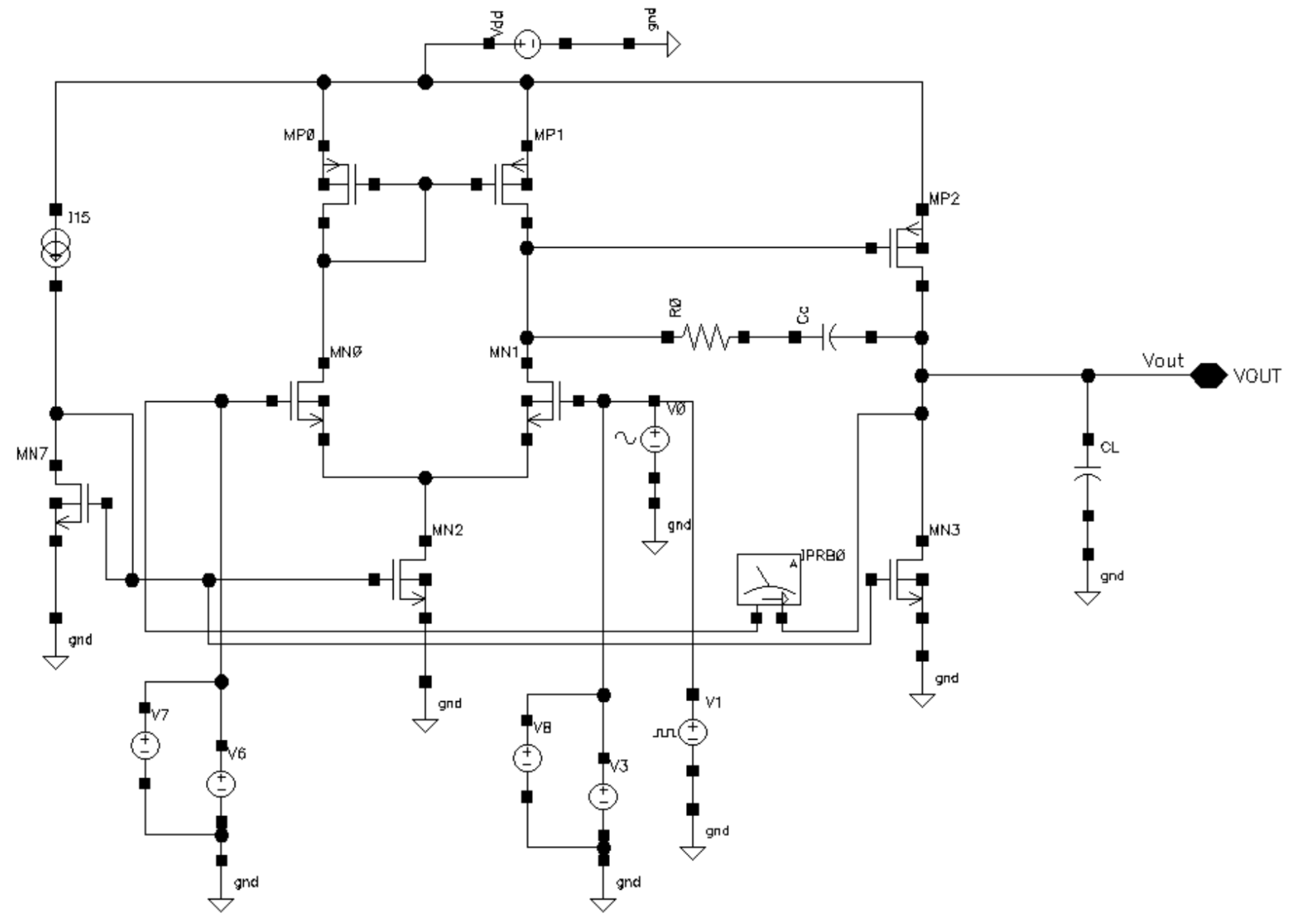
The first stage employs the classic 5-transistor OTA to provide high gain, while the second stage uses a PMOS common-source amplifier to achieve large output swing. There is an inherent stability challenge between the two stages—each pole contributes 90° phase shift, and improper design leads to oscillation.
Key design decisions:
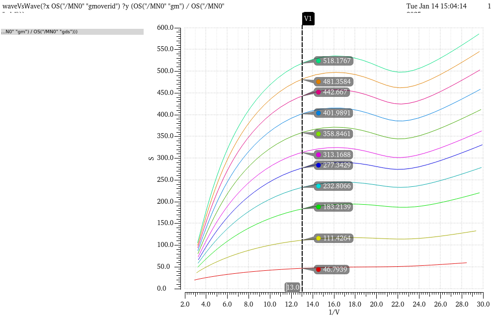
- Precisely selected L=1.4μm (NMOS) and L=1.8μm (PMOS) via gm/ID curves, achieving the optimal trade-off between gain and speed
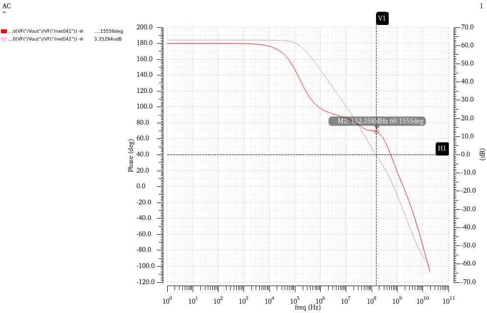
- Introduced Miller compensation + nulling resistor Rz, achieving a final phase margin of 69°
- Amplifier transistors gm/ID=13 (low noise), current source transistors gm/ID=8 (high output impedance)
Final results: power 480μW | slew rate 152V/μs | output swing 1568mV—far exceeding the 800mV specification.
Approach 2: Folded Cascode — Single-Stage High Bandwidth
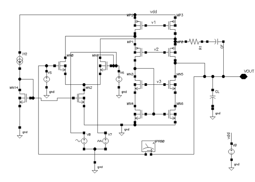
The folded cascode achieves high gain at lower supply voltages through clever current reuse. Building on a precise mathematical model, this project introduces two major optimizations:
- Wide-swing current mirrors replace simple voltage-source biasing, ensuring all transistors operate precisely in saturation and resolving insufficient swing issues
- RC feedback network fine-tunes the gain-bandwidth balance, compensating for bandwidth loss caused by parasitic effects
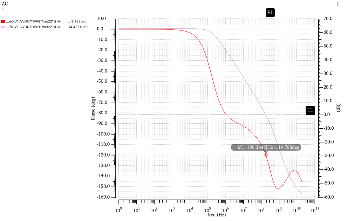
The single-stage structure is inherently stable, requiring no complex frequency compensation. Final results: power only 406μW | bandwidth 190MHz | gain 62.8dB.
Performance Comparison Overview
| Parameter | Specification Requirement | 5T-OTA Two-Stage Op-Amp | Folded Cascode |
|---|---|---|---|
| Differential Gain | > 60dB | 63.0dB | 62.8dB |
| Unity-Gain Bandwidth | > 100MHz | 149MHz | 190MHz |
| Phase Margin | > 60° | 69.3° | 60.2° |
| Slew Rate (Up) | > 10V/μs | 152V/μs | 78.1V/μs |
| Output Swing | > 800mV | 1568mV | 858mV |
| Power Consumption | As low as possible | 480μW | 406μW |
Project Takeaways and Skill Accumulation
This project gave me a deep appreciation for the true meaning of "design is about trade-offs" in analog IC design. Gain vs bandwidth, speed vs power, stability vs complexity—there is no absolute optimal solution, only the best trade-off for a specific scenario.
Core Competencies:
- Proficient use of the gm/ID design methodology, mastering device characterization simulation and design decision-making in the Cadence Virtuoso environment
- In-depth understanding of frequency compensation (Miller compensation / nulling resistor) and bias circuit design (wide-swing current mirrors)
- Independently completed the full design loop: specification decomposition → hand calculation → simulation verification → iterative optimization
- Able to select the appropriate architecture (high-gain large dynamic range vs low-power high-speed) based on application scenarios and perform targeted optimization
Comments