PN Junction Diode Simulation and Characterization Using Silvaco ATLAS
In a microelectronics fundamentals course, we used Silvaco ATLAS to perform complete device modeling and characteristic simulation of a PN junction diode, covering forward I-V characteristics, breakdown characteristics, electric field distribution, and energy band structure analysis.
1. Simulation Methodology
We defined a one-dimensional PN junction structure in ATLAS: mesh definition → region definition → electrode setup → doping profile → solver configuration. The simulation script is as follows:
# Mesh definition\nmesh space.mult=1.0\nx.mesh loc=0.00 spac=0.1\nx.mesh loc=5.00 spac=0.1\n\n# Regions and electrodes\nregion number=1 x.min=0 x.max=5 material=Silicon\nelectrode top name=anode\nelectrode bottom name=cathode\n\n# Doping profile\ndoping uniform conc=5e+16 n.type\ndoping gaussian junction=1 conc=5e+17 n.type\n\n# Output structure\nstructure outfile=task3.str\ntonyplot init\n\n# Solver\nmethod newton\nlog outfile=task3.log\nsolve vanode=0 vstep=0.05 vfinal=3.0 name=anode\n\n# Visualization\ntonyplot task3.logKey parameters: anode voltage swept from 0V to 3V (0.05V step), using Newton iteration to solve the semiconductor equations. The doping uses a uniform background doping (5×10¹⁶ cm⁻³) with a Gaussian surface doping overlay (5×10¹⁷ cm⁻³), forming a one-sided abrupt junction structure.
2. Simulation Results
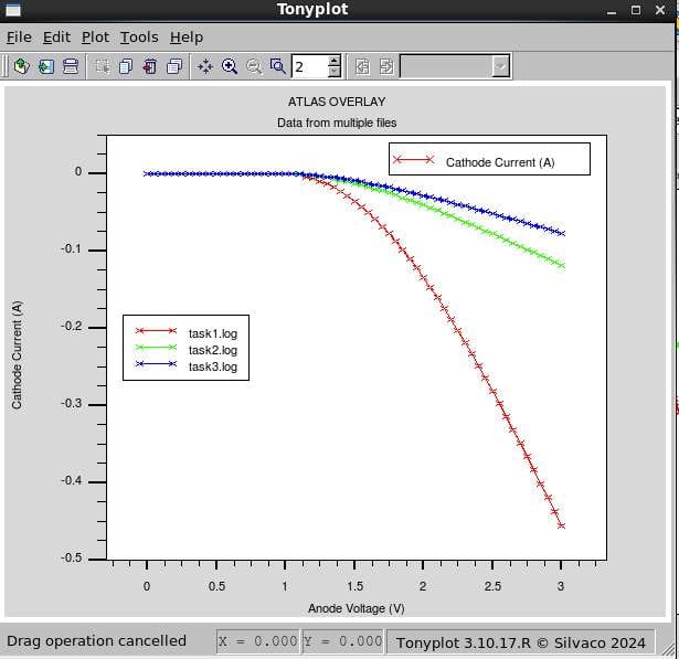
I-V Characteristics
The forward I-V curve fully demonstrates the typical behavior of a diode: extremely low current in the low-bias region (off state), followed by exponential current growth after approximately 0.7V (on state), consistent with the predictions of the ideal diode equation I = I₀(e^(qV/kT) − 1). Comparison of three curves under different doping concentrations validates the effect of doping on forward voltage drop and on-resistance.
Doping Distribution and Electric Field
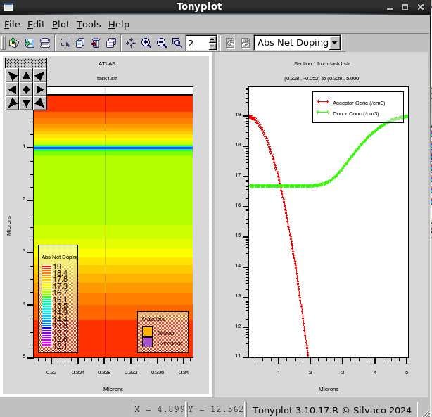
The doping distribution plot clearly illustrates the space charge region of the PN junction: near the metallurgical junction, acceptor and donor concentrations intersect, forming the depletion region. The electric field peaks at the junction interface, and the energy bands bend in this region—this is precisely the physical origin of the diode's unidirectional conductivity.
3. Summary
Through Silvaco ATLAS's complete device simulation workflow—mesh definition → doping modeling → numerical solving → result visualization—we gained a physics-level understanding of the PN junction's operating mechanism, rather than remaining at the equivalent circuit model level. The code is reusable; adjusting parameters such as doping concentration and junction depth allows rapid exploration of different device designs.
Comments