一个简单的CMOS结构的Athena仿真以及代码解析
仿真
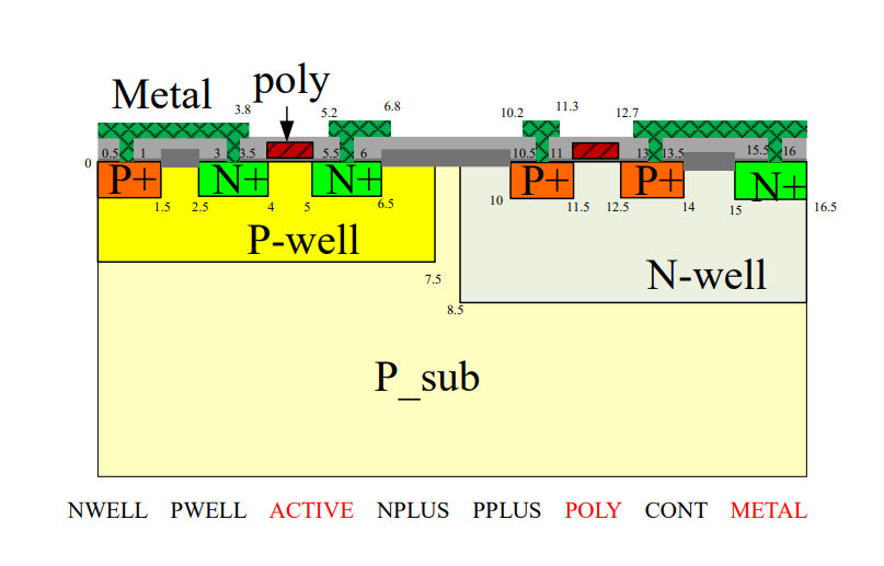
期末项目要用Athena做一个CMOS制造流程,结构如图。
仿真结果:
仿真数值:
Extracted parameters(The data must be clearly given, and the screenshots are needed for prove)
The step 5, extract the nwell junction depth 05nwell = 0.742309um
The step 7, extract the thickness of SiO2 inside Nwell 07tox_in_nwell = 0.210375um
The step 7, extract the thickness of SiO2 outside Nwell 07tox_out_nwell = 0.243607um
The step 7, step height of silicon surface = 0.178331-0.114659 um = 0.063672um
The step 7, extract the junction depth of Nwell 07nwell = 4.45937um
The step 9, extract the thickness of SiO2 inside Nwell 09tox_in_nwell = 0.0430882um
The step 9, extract the thickness of SiO2 outside Nwell 09tox_out_nwell = 0.0430863um
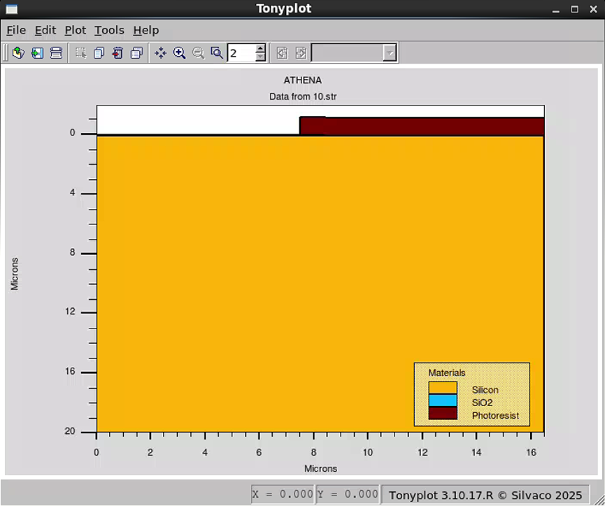
Step 10, observe the photoresist
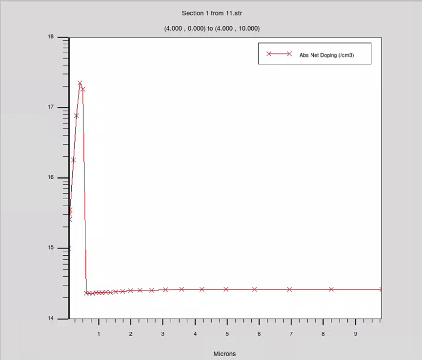
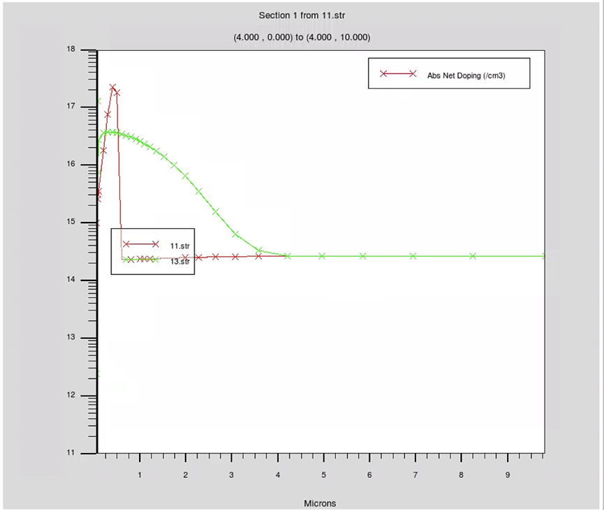
Step 11, curve of Boron concentration, x axis for 1D curve range 0-10
Step 13, plot curve1 and 2 in one picture x axis range 0-10
The step 15, extract thickness of SiO2 in the active region 15thickness_of_SiO2_in_active_region = 0.0421572um
The step 20, extract thickness of SiO2(X.val=8) 20SiO2 = 0.951967um
The step 22, due to the step 20, thickness of SiO2 needs to be etched is about 0.15um, extract remained thickness of SiO2 22SiO2 = 0.801967um
The step 23, extract thickness of SiO2 X=4.5 23SiO2 = 0.0335531um
The step 28, thickness of oxide on top of NMOS Poly and PMOS Poly 28NpolySiO2 = 0.0125231um 28PpolySiO2 = 0.0125231um
The step 31, extract junction depth of N+, x = 3.5 31N+1 = 0.266465um, x = 5.5 31N+2 = 0.265963um
The step 33, extract thickness of oxide on top of NMOS Poly and PMOS Poly 33Npoly = 0.0200301um 33Ppoly = 0.0322859um
The step 36, extract junction depth of P+, x = 11 36P+1 = 0.303582um, x=13 36P+2 = 0.29539um
The step 47,
1. Vt for NMOS with Vsub=2V; 47NVt = 2.48013V
2. Vt for PMOS with Vsub=0V; 47PVt = -1.6258V
3. Channel doping for NMOS and PMOS; 47NChannelDoping = 2.71413e+15 atoms/cm3, 47PChannelDoping = 1.47776e+16 atoms/cm3.
4. Gate oxide thickness for NMOS and PMOS 47Noxide = 0.0335536um, 0.0335637um.
下面是我的仿真代码:
go athena

#00
line x location=0 spacing=0.1
line x location=16.5 spacing=0.1
line y location=0 spacing=0.1
line y location=1 spacing=0.1
line y location=20 spacing=5

#01
init silicon boron resistivity=50 orientation=100 two.d

#02
deposit oxide thick=0.1

structure outfile=02.str

#03
deposit photoresist thick=1.2

#
etch photoresist right p1.x=8.5

structure outfile=03.str

#04
etch oxide
structure outfile=04.str

#05
#
implant phosphor dose=5.0e12 energy=130  crystal

#
extract name="05nwell" xj material="Silicon" mat.occno=1 x.val=12 junc.occno=1

structure outfile=05.str

#06
etch photoresist all

#07

#
diffus time=15 minutes temp=800 f.o2=8
#
diffus time=60 minutes temp=800 t.final=1180  f.o2=8
#
diffus time=200 minutes temp=1180 f.n2=8 f.o2=4
#
diffus time=120 minutes temp=1180 t.final=800 f.n2=8
#
diffus time=15 minutes temp=800 f.n2=6

# Extract thickness
extract name="07tox_in_nwell" thickness material="SiO2" mat.occno=1 x.val=12.0
#
extract name="07tox_out_nwell" thickness material="SiO2" mat.occno=1 x.val=4.0

#
extract name="07Silicon_inside_Nwell_surface" min.bound material="SiO2" mat.occno=1 x.val=12.0

extract name="07Silicon_outside_Nwell_surface" min.bound material="SiO2" mat.occno=1 x.val=4.0
#
extract name="07nwell" xj material="Silicon" mat.occno=1 x.val=12

#08
etch oxide all

structure outfile=08.str

#09
#
diffus time=34 minutes temp=800 f.n2=8
#
diffus time=25 minutes temp=800 t.final=1000  f.n2=8
#
diffus time=5 minutes temp=1000 f.n2=8
#
diffus time=45 minutes temp=1000 f.o2=8
#
diffus time=30 seconds temp=1000 f.o2=8
#
diffus time=20 minutes temp=1000 t.final=900  f.n2=8
#
diffus time=30 minutes temp=900 f.n2=8
#
diffus time=1 hours temp=900 t.final=800  f.n2=8
#
diffus time=15 minutes temp=800 f.n2=8
#
extract name="09tox_in_nwell" thickness material="SiO2" mat.occno=1 x.val=12.0
#
extract name="09tox_out_nwell" thickness material="SiO2" mat.occno=1 x.val=4.0
#
structure outfile=09.str
#10
#
deposit photoresist thick=1.2
#
etch photoresist left p1.x=7.5

structure outfile=10.str
#11
#
implant boron dose=5.0e12 energy=110 crystal
#
structure outfile=11.str
#12
#
etch photoresist all
#13
#
diffus time=20 minutes temp=800 f.n2=8
#
diffus time=60 minutes temp=800 t.final=1150  f.n2=8
#
diffus time=150 minutes temp=1150 f.n2=8
#
diffus time=120 minutes temp=1150 t.final=800  f.n2=8
#
diffus time=15 minutes temp=800 f.n2=6
#
structure outfile=13.str
#14
#
etch oxide all
#15
#
diffus time=34 minutes temp=800 f.n2=8
#
diffus time=25 minutes temp=800 t.final=1000  f.n2=8
#
diffus time=5 minutes temp=1000 f.n2=8
#
diffus time=45 minutes temp=1000 f.o2=8
#
diffus time=30 seconds temp=1000 f.o2=8
#
diffus time=20 minutes temp=1000 t.final=900  f.n2=8
#
diffus time=30 minutes temp=900 f.n2=8
#
diffus time=1 hours temp=900 t.final=800  f.n2=8
#
diffus time=15 minutes temp=800 f.n2=8
#
extract name="15thickness_of_SiO2_in_active_region" thickness material="SiO2" mat.occno=1 x.val=4.5
#
structure outfile=15.str
#16
#
deposit nitride thick=0.15 div=5
#
structure outfile=16.str
#17
#18
#
etch nitride start x=1.50 y=3.00
etch cont x=2.50 y=3.00
etch cont x=2.50 y=-2.00
etch done x=1.50 y=-2.00
#
etch nitride start x=6.50 y=3.00
etch cont x=10.00 y=3.00
etch cont x=10.00 y=-2.00
etch done x=6.50 y=-2.00
#
etch nitride start x=14.00 y=3.00
etch cont x=15.00 y=3.00
etch cont x=15.00 y=-2.00
etch done x=14.00 y=-2.00
#
structure outfile=18.str
#19
#20
#
diffus time=30 minutes temp=800 f.n2=20
#
diffus time=8 minutes temp=800 t.final=950  f.n2=8
#
diffus time=1 hours temp=950 f.n2=8
#
diffus time=15 minutes temp=950 f.o2=8
#
diffus time=30 seconds temp=950 f.o2=8
#
diffus time=6 hours temp=950 f.h2=7.3 f.o2=4
#
diffus time=50 minutes temp=950 t.final=800  f.n2=8
#
diffus time=10 minutes temp=800 t.final=750  f.n2=8
#
diffus time=15 minutes temp=750 f.n2=10
extract name="20SiO2" thickness material="SiO2" mat.occno=1 x.val=8.0
#
structure outfile=20.str
#21
#
etch nitride all
#
structure outfile=21.str
#22
#
etch oxide dry thick=0.15
#
structure outfile=22.str
extract name="22SiO2" thickness material="SiO2" mat.occno=1 x.val=8.0
#23
#
diffus time=20 minutes temp=750 t.final=1000  f.n2=3
#
diffus time=33 minutes temp=1000 dryo2
#
diffus time=20 minutes temp=1000 t.final=750  inert
#
extract name="23SiO2" thickness material="SiO2" mat.occno=1 x.val=4.5
structure outfile=23.str
#24
#
deposit polysilicon thick=0.35 c.phosphor=5e12 div=5
structure outfile=24.str
#25
#26
#
etch polysilicon start x=0.00 y=2.00
etch cont x=4.00 y=2.00
etch cont x=4.00 y=-1.00
etch done x=0.00 y=-1.00
#
etch polysilicon start x=5.00 y=2.00
etch cont x=11.50 y=2.00
etch cont x=11.50 y=-1.00
etch done x=5.00 y=-1.00
structure outfile=26.str
#
etch polysilicon start x=12.50 y=2.00
etch cont x=16.50 y=2.00
etch cont x=16.50 y=-1.00
etch done x=12.50 y=-1.00
structure outfile=26.str

#27
#28
#
diffus time=18 minutes temp=800 f.n2=8
#
diffus time=15 minutes temp=800 f.n2=8
#
diffus time=15 minutes temp=800 t.final=900  f.n2=8
#
diffus time=15 minutes temp=900 f.hcl=0.1 f.o2=8
#
diffus time=30 seconds temp=900 f.hcl=0.1 f.o2=8
#
diffus time=3 minutes temp=900 f.o2=8
#
diffus time=30 minutes temp=900 t.final=800  f.n2=8
#
diffus time=15 minutes temp=800 f.n2=15

structure outfile=28.str
#
extract name="28NpolySiO2" thickness material="SiO2" mat.occno=1 x.val=4.5
#
extract name="28PpolySiO2" thickness material="SiO2" mat.occno=1 x.val=12

#
init infile=28.str

#29
deposit photoresist thick=1.2
#
etch photoresist start x=15.50 y=2.00
etch cont x=15.50 y=-2.00
etch cont x=16.50 y=-2.00
etch done x=16.50 y=2.00

etch photoresist start x=3.00 y=2.00
etch cont x=3.00 y=-2.00
etch cont x=6.00 y=-2.00
etch done x=6.00 y=2.00

structure outfile=29.str

#30
#31
#
implant arsenic dose=5.0e15 energy=80 crystal

#
extract name="31N+1" xj material="Silicon" mat.occno=1 x.val=3.5 junc.occno=1
#
extract name="31N+2" xj material="Silicon" mat.occno=1 x.val=5.5 junc.occno=1


structure outfile=31.str
#32
#
etch photoresist all

structure outfile=32.str
#33
#
diffus time=18 minutes temp=800 f.n2=8
#
diffus time=15 minutes temp=800 f.n2=8
#
diffus time=15 minutes temp=800 t.final=900  f.n2=8
#
diffus time=15 minutes temp=900 f.hcl=0.1 f.o2=8
#
diffus time=30 seconds temp=900 f.hcl=0.1 f.o2=8
#
diffus time=3 minutes temp=900 f.o2=8
#
diffus time=30 minutes temp=900 t.final=800  f.n2=8
#
diffus time=15 minutes temp=800 f.n2=15

#
extract name="33Npoly" thickness material="SiO2" mat.occno=1 x.val=4.5
#
extract name="33Ppoly" thickness material="SiO2" mat.occno=1 x.val=12

structure outfile=33.str
#34
deposit photoresist thick=1.2
#
etch photoresist start x=0.00 y=2.00
etch cont x=0.00 y=-2.00
etch cont x=1.00 y=-2.00
etch done x=1.00 y=2.00

etch photoresist start x=10.5 y=2.00
etch cont x=10.5 y=-2.00
etch cont x=13.5 y=-2.00
etch done x=13.5 y=2.00

structure outfile=34.str

#35
#36
#
implant bf2 dose=4.0e15 energy=80 crystal
#
#
extract name="36P+1" xj material="Silicon" mat.occno=1 x.val=11 junc.occno=1
#
extract name="36P+2" xj material="Silicon" mat.occno=1 x.val=13 junc.occno=1

structure outfile=36.str

#37
#
etch photoresist all

structure outfile=37.str
#38
#
deposit oxide thick=1

structure outfile=38.str
#39
#40
#41
#
etch oxide start x=0.50 y=2.00
etch cont x=0.50 y=-2.00
etch cont x=1.00 y=-2.00
etch done x=1.00 y=2.00
#
etch oxide start x=3.00 y=2.00
etch cont x=3.00 y=-2.00
etch cont x=3.50 y=-2.00
etch done x=3.50 y=2.00
#
etch oxide start x=5.50 y=2.00
etch cont x=5.50 y=-2.00
etch cont x=6.00 y=-2.00
etch done x=6.00 y=2.00
#
etch oxide start x=10.50 y=2.00
etch cont x=10.50 y=-2.00
etch cont x=11.00 y=-2.00
etch done x=11.00 y=2.00
#
etch oxide start x=13.00 y=2.00
etch cont x=13.00 y=-2.00
etch cont x=13.50 y=-2.00
etch done x=13.50 y=2.00
#
etch oxide start x=15.50 y=2.00
etch cont x=15.50 y=-2.00
etch cont x=16.00 y=-2.00
etch done x=16.00 y=2.00

structure outfile=41.str
#42
#43
#44
#
deposit aluminum thick=1.45
structure outfile=45.str
#45
#46
#
etch aluminum start x=3.80 y=2.00
etch cont x=3.80 y=-10.00
etch cont x=5.20 y=-10.00
etch done x=5.20 y=2.00
#
etch aluminum start x=6.80 y=2.00
etch cont x=6.80 y=-10.00
etch cont x=10.20 y=-10.00
etch done x=10.20 y=2.00
#
etch aluminum start x=11.30 y=2.00
etch cont x=11.30 y=-10.00
etch cont x=12.70 y=-10.00
etch done x=12.70 y=2.00

structure outfile=46.str
#47
extract name="47NVt" 1dvt ntype vb=2.0 x.val=4.5
extract name="47PVt" 1dvt ptype vb=0 x.val=12
extract name="47NChannelDoping" surf.conc impurity="Net Doping" material="Silicon" mat.occno=1 x.val=4.5
extract name="47PChannelDoping" surf.conc impurity="Net Doping" material="Silicon" mat.occno=1 x.val=12
extract name="47Noxide" thickness material="SiO2" mat.occno=2 x.val=4.5
extract name="47Poxide" thickness material="SiO2" mat.occno=2 x.val=12
这段代码模拟了一个典型的CMOS制造流程,从最初的硅衬底开始,经过掺杂、氧化、刻蚀、沉积等一系列步骤,最终形成具有基本功能的晶体管结构。
代码解析
让我们一步步剖析代码中的关键部分:
1. 准备阶段 (#00, #01)
go athena: 启动 Athena 工艺仿真器。line: 定义了仿真的二维区域和网格密度。注意要表面较密。init silicon boron resistivity=50 orientation=100 two.d: 初始化仿真基底。我们从一块掺硼(P型)、电阻率为50欧姆-厘米、晶向为(100)的硅衬底开始。这是最常见的CMOS起始材料。
2. N阱形成 (#02 - #08)
deposit oxide thick=0.1: 沉积一层薄氧化层,可能作为后续注入的缓冲层或牺牲层。deposit photoresist thick=1.2: 沉积光刻胶。etch photoresist right p1.x=8.5: 刻蚀掉坐标 x=8.5 右侧的光刻胶。左侧的光刻胶保留,形成掩模。etch oxide: 刻蚀掉光刻胶下方(右侧)暴露的氧化层。implant phosphor dose=5.0e12 energy=130 crystal: 在暴露区域注入磷(Phosphor)。磷是N型掺杂剂。这次注入将在P型衬底中形成N型区域,也就是N阱。剂量和能量决定了注入的浓度和深度。crystal参数表示考虑了晶体效应。extract name="05nwell" xj ...: 测量注入后N阱的结深(Junction Depth, xj)。etch photoresist all: 移除剩余的光刻胶。diffus ...: 接下来是一系列长时间、高温的扩散(Diffusion)步骤,温度从800°C升至1180°C,并在不同气氛(O2, N2)下进行。这些步骤的作用是:- 激活注入的磷,使其具有电活性。
- 将磷原子向硅内部和横向扩散,形成更深、更宽的N阱。
- 在有O2的地方可能伴随氧化层生长。
extract ...: 在扩散后再次测量N阱结深、氧化层厚度等参数,以检查扩散效果。etch oxide all: 移除扩散后生成的或剩余的氧化层。
3. 场氧化层 (LOCOS) 形成 (#09 - #21)
diffus ...: 又一系列扩散步骤,可能用于生长一层薄的垫氧化层(Pad Oxide)。deposit nitride thick=0.15: 沉积一层氮化硅(Nitride)。氮化硅在高温氧化时可以阻挡氧原子扩散,常被用作局部氧化(LOCOS)的掩模。etch nitride start ... done ...: 通过精确的坐标定义,刻蚀掉氮化硅层,在未来需要形成晶体管“有源区”的地方露出下层结构。未刻蚀掉的氮化硅区域将对应未来的“场区”,形成厚隔离氧化层。diffus ... f.h2=7.3 f.o2=4: 长时间的高温扩散(950°C),特别注意f.h2和f.o2参数,这代表了湿氧气氛,是典型的场氧化工艺条件。在没有氮化硅掩盖的区域,硅会大量氧化,形成很厚的场氧化层(Field Oxide, FOX),用于隔离不同的器件。extract ...: 测量场氧化层厚度。etch nitride all: 移除剩余的氮化硅掩模。
4. 栅极形成 (#22 - #26)
etch oxide dry thick=0.15: 刻蚀掉部分氧化层,可能是在有源区清理表面。diffus ... dryo2: 短时间高温(1000°C)干氧扩散。这是生长薄栅氧化层(Gate Oxide)的关键步骤。栅氧化层是栅电极和硅衬底之间的绝缘层。extract ...: 测量栅氧化层厚度。deposit polysilicon thick=0.35 c.phosphor=5e12: 沉积一层掺磷(N型)的多晶硅(Polysilicon)。多晶硅是现代CMOS器件常用的栅电极材料。etch polysilicon start ... done ...: 刻蚀多晶硅层,形成独立的栅极结构。
5. 源/漏区形成 (#27 - #37)
diffus ...: 短时间的退火步骤,可能用于稳定栅极或生长一层薄钝化氧化层。extract ...: 测量多晶硅上的氧化层厚度。init infile=28.str: 读取上一步保存的结构文件,确保从正确状态开始下一步。deposit photoresist thick=1.2: 沉积光刻胶。etch photoresist start ... done ...: 刻蚀光刻胶,暴露出需要形成N+源/漏的区域。请注意,栅极多晶硅也同时起到了掩模作用(自对准工艺)。implant arsenic dose=5.0e15 energy=80 crystal: 注入砷(Arsenic)。砷是N型掺杂剂,剂量很高(5e15),用于形成高浓度N+区。这将在P型衬底(左侧区域)栅极两侧形成NMOS的源/漏区。extract ... xj ...: 测量N+源/漏的结深。etch photoresist all: 移除光刻胶。diffus ...: 退火步骤,激活N+掺杂。deposit photoresist ... etch photoresist ...: 再次沉积和刻蚀光刻胶,暴露出需要形成P+源/漏的区域。implant bf2 dose=4.0e15 energy=80 crystal: 注入BF2。BF2分解后注入硼(Boron),硼是P型掺杂剂。这将在N阱区域(右侧区域)栅极两侧形成PMOS的P+源/漏区。extract ... xj ...: 测量P+源/漏的结深。etch photoresist all: 移除光刻胶。
6. 互连层形成 (#38 - #46)
deposit oxide thick=1: 沉积一层厚的氧化层,作为层间介质(Interlayer Dielectric, ILD),用于隔离金属层和下层结构。etch oxide start ... done ...: 刻蚀出接触孔(Contact Holes),露出源/漏区和栅极上需要连接金属的区域。deposit aluminum thick=1.45: 沉积一层铝。铝是常见的金属互连材料。etch aluminum start ... done ...: 刻蚀铝层,形成金属连线(Metal Interconnects),通过接触孔连接到下层器件的源/漏和栅极。
7. 参数提取与分析 (#47)
extract name="47NVt" 1dvt ntype vb=2.0 x.val=4.5: 提取NMOS晶体管(位于x=4.5附近)在一定衬底偏压下的阈值电压(Vt)。extract name="47PVt" 1dvt ptype vb=0 x.val=12: 提取PMOS晶体管(位于x=12附近)的阈值电压。extract name="47NChannelDoping" surf.conc ...: 提取NMOS沟道区域的表面净掺杂浓度。extract name="47PChannelDoping" surf.conc ...: 提取PMOS沟道区域的表面净掺杂浓度。extract name="47Noxide" thickness ...: 提取NMOS栅极下方的栅氧化层厚度。extract name="47Poxide" thickness ...: 提取PMOS栅极下方的栅氧化层厚度。
这些提取的参数是评估仿真结果是否符合设计要求的关键指标。
总结
通过这段不到300行的Athena代码,我们模拟了CMOS制造的核心流程:N阱形成、场氧化隔离、栅极制作、源/漏注入和退火、以及最后的金属互连。每一个命令都对应着半导体工厂中的一项实际工艺步骤。
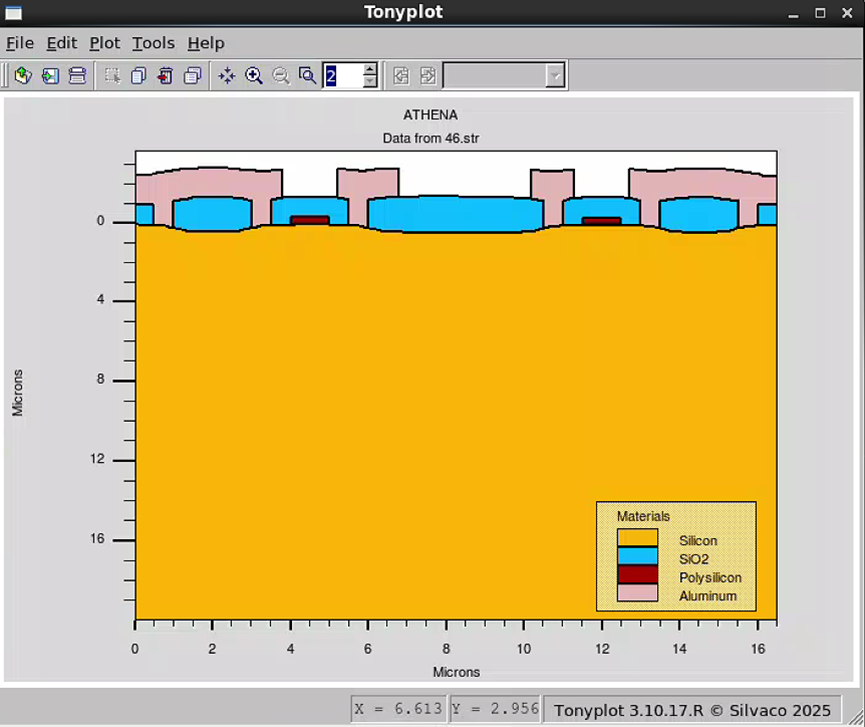
代码中的 structure outfile=XX.str 命令会在每一步之后保存当前的结构文件,这些文件可以在 Athena 的可视化工具 DeckBuild 中打开,看到器件结构随工艺进行而发生的变化,例如掺杂区域的扩散、氧化层的生长、刻蚀形成的图案等等。
工艺模拟是现代集成电路设计和制造中不可或缺的环节。它不仅可以帮助工程师理解复杂的物理化学过程,预测工艺变化对器件性能的影响,还能在投入昂贵的实际生产之前,进行大量的实验和优化,大大缩短开发周期,降低成本。
Comments